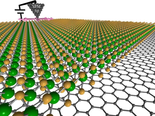
Two-dimensional materials just a few atoms thick have special quantum mechanical properties. What often makes these materials special: their defects. But there are a huge number of potential defects, and they aren’t all useful. To sift for useful defects, researchers have developed an automated method to analyze an important part of the 2D materials puzzle: how matter interacts with electromagnetic radiation. The method combines scanning tunneling microscopy with AI to map atomic and electronic features.
The method opens the door to the detailed exploration of novel materials, including quantum materials. The techniques and software could be extended to other techniques in scanning probe microscopy. The researchers have summarized the method in a user-friendly, open access, and tailorable software package.
