Intel released a novel transistor last year, the Tri-Gate, which replaced a two-dimensional flat planar gate with a 3-D silicon fin. This “reinvention of the transistor,” Intel announced, would increase performance up to 37 percent at low voltage. At 22 nanometers, it was 10 nm smaller than the current state-of-the-art transistor.
Such advancements keep Intel on the pace of improvement Moore’s law predicted and promises a host of applications, from computational devices to arrays of environmental and medical sensors.
This latest advance was made possible, in part, by the Network for Computational Nanotechnology (NCN). Started almost 10 years ago at Purdue University under the direction of Mark Lundstrom and Gerhard Klimeck, NCN is home to nanoHUB (www.nanohub.org).
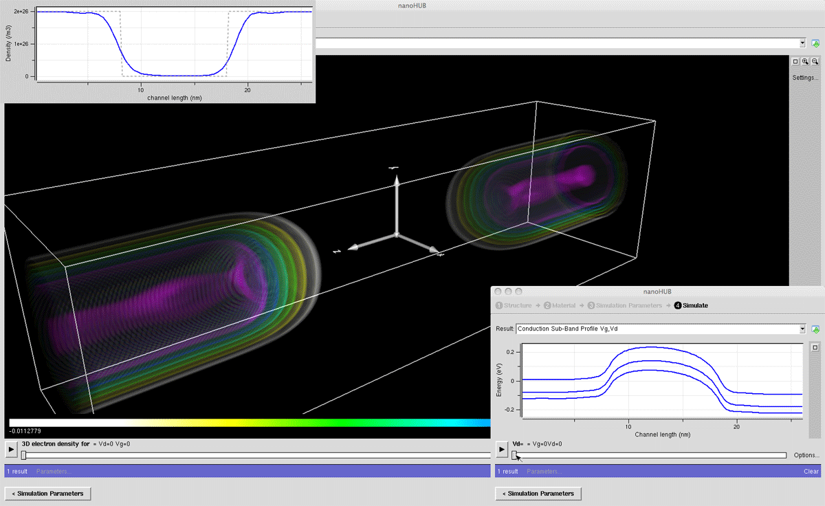
The Klimeck group has been building a suite of nanoelectronic modeling tools called NEMO/OMEN. They’ve used the tools to model various devices, including finFETs, the fin-featuring transistors. (FET: field effect transistor.) The OMEN code has demonstrated almost perfect parallel scaling while exceeding performance of a petaflops, or quadrillion computations a second, on a high-performance computer.
Klimeck models quantum mechanical electron flow in nanoscale devices’ transistors and semiconductors. The models have grown, from portraying a few hundred atoms when he started his research at Texas Instruments in 1994 to 100 million atoms today.
The Department of Energy’s INCITE (Innovative and Novel Computational Impact on Theory and Experiment) program has granted Klimeck 15 million processor hours on Jaguar, the Cray XT5 at Oak Ridge National Laboratory. Jaguar is one of only a few computers that operate at the petascale. OMEN, for example, has scaled to a whopping 221,400 of Jaguar’s 224,000 processor cores with a sustained performance above 1 petaflops.
The research team’s paper reporting the simulation received an honorable mention in competition for the prestigious Gordon Bell Prize at the SC11 high-performance computing conference in Seattle this past November. The prize recognizes the world’s most advanced scientific computing application.
The team’s paper described double-precision calculations of two two-dimensional nanoelectric devices, achieving 1.27 petaflops for one and 1.28 petaflops for another. A mixed single- and double-precision calculation of one of the devices reached 1.44 petaflops.
That kind of power “allows us to run more extended structures and to address problems that we couldn’t technically scale to on the computers we have available at Purdue,” Klimeck says.
His goals for running the NEMO and OMEN codes on Jaguar include developing new technologies for even faster nanoscale switches and smaller devices with reduced heat generation.
Until about five years ago, the electronics industry made smaller and smaller devices that also ran faster and faster. This created a big challenge: On the one hand, smaller transistors that can run faster also leak more electrons. The energy lost to leakage tends to overheat the transistor. On the other hand, deliberately running at less than peak speed requires less energy and creates less heat, creating a speed/heat stalemate.
One way to sidestep this stalemate is to reduce the transistor’s operating voltage so that leaking electrons carry less energy. The lowest energy today’s transistors use is 0.9 volts. The hope is to reduce that by one-quarter to one-half. Numerous research groups are exploring alternative transistors theorized to be more energy efficient.
Klimeck hopes his revamped NEMO and OMEN codes and Jaguar can help explore these kinds of transistors and point to better design ideas.
The road to NEMO
Klimeck joined NCN as technical director in 2003. Earlier in his career, at Texas Instruments, his team was the first to build a quantum transport simulator to model electron flow through a resonant tunneling diode (RTD).
In the late 1990s, he and others considered the RTD as a way to boost chip performance should silicon “run out of steam,” Klimeck says. “But silicon kept scaling despite all predictions that it could not.”
Still, the RTD “guided our fundamental understanding of electron flow at the nanometer scale,” Klimeck says. In an RTD, electrons are confined in one dimension. In studying the RTD, Klimeck and his collaborators wrote the code for his NEMO 1-D (nanoelectronic modeling) software, realizing “that we had to represent the material by one atomic monolayer at a time. In this one-dimensional representation, we had basically a chain of atoms like a string of pearls. In the cross section, which was very, very large, we would imagine along the pearls blue ones, red ones, each one an atom of a different flavor. That was the key insight I learned, that we’d have to represent things atomistically, but we couldn’t afford to compute electron flow through these structures that might contain a million atoms in a 3-D distribution.”
“Today’s research devices such as finFETs, nanowires, nanotubes, graphene, and optical detectors are topologically all the same to me, meaning they are atoms connected to each other, and typically connected to a source on one end and a drain on another, with a valve or gate around them.”
Klimeck left TI in 1998 and joined NASA’s Jet Propulsion Laboratory to work on quantum dots. Quantum dots behave like artificial atoms that confine a few additional electrons on the length scale of a few tens of nanometers.
“These quantum dot geometries can be dome-shaped, even pyramidal,” Klimeck says. “They are of interest for optical detectors and lasers. The way that nano researchers form quantum dots is to take some low band-gap material, that’s indium arsenide, and surround it with a higher band-gap material, gallium arsenide. The electrons in this structure will accumulate in the lower band-gap material. Once there, they will zoom around the dome in orbits much like electron orbits around the nucleus of a single atom. The dome, containing millions of atoms, nonetheless acts like a single atom, but an artificial atom with behavior that can be designed.”
To model these devices in 3-D space, he and his colleagues wrote NEMO 3-D, which by 2005 had the capability to model 50-million-atom quantum dot structures. Quantum dots offer the promise of controlling the discrete energies of these atoms, which means they can be used to examine various spectral energies and can be tuned to respond to certain spectral lines. NASA JPL is interested in them to search for water or minerals and other matter in space. They also hold potential as sensors for carbon dioxide emissions and aerosols.
In recent years, two of Klimeck’s graduate students, Hoon Ryu and Sunhee Lee, rewrote NEMO 3-D to run on petascale machines, “so we could scale to 30,000 to 40,000 cores, letting us do more extensive quantum dots,” he says.
Not long after coming to Purdue, Klimeck engaged Mathieu Luisier at the Swiss Federal Institute of Technology (ETH) with his group to build from scratch the combination of NEMO 1-D and NEMO 3-D so Klimeck’s group could closely examine nanowires and ultra-thin body transistors, tracking the current flow in them. Ultimately, Klimeck, Luisier and others dubbed the combined software OMEN – NEMO backwards.
“We kind of said, let’s do it one more time, backwards,” Klimeck says with a chuckle. “NEMO 1-D was doing really well on electron flow, but its limitation was that it essentially depicted a string of atoms. NEMO 3-D did really well in terms of millions of atoms, but it could not really simulate electron flow. OMEN combines the two in such a way that it can calculate, say, 100,000 atoms while considering the electron flow through geometries defined by those 100,000 atoms.”
But to do fabrications and analyses that, besides electron transport, involve atomistic representations plus electronic structure, researchers are tackling what a physicist would call non-equilibrium quantum statistical mechanics, and that, Klimeck says, “is one of the hardest things you can imagine doing computationally.”